- Aluminum PCB Capability
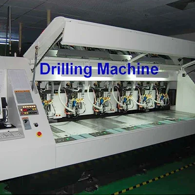
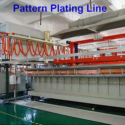
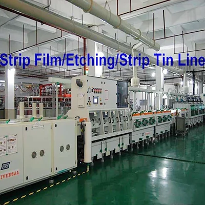
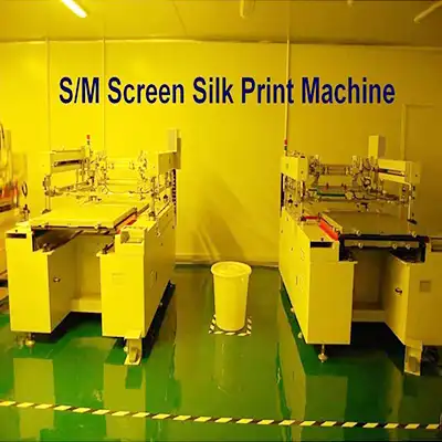
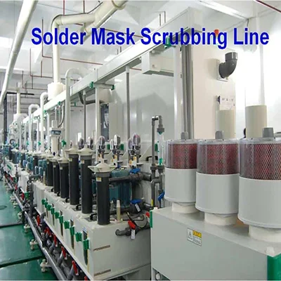
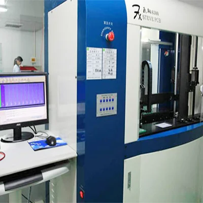
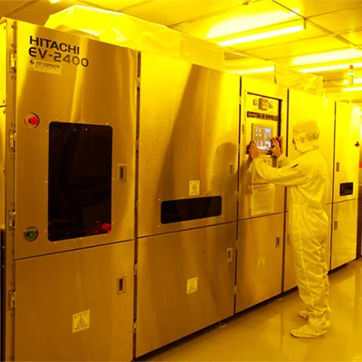
- PCB manufacturing equipment
Introducing our LED PCB, specifically designed to meet the unique requirements of LED lighting applications. Our LED PCBs are engineered to provide excellent thermal management, efficient power distribution, and optimal performance for LEDs.
Our LED PCBs feature a combination of specialized materials, advanced circuit design, and thermal management techniques to maximize the performance and lifespan of LED lighting systems.
Whether you’re working on LED light bulbs, strips, panels, or other lighting applications, our LED PCBs offer the reliability and efficiency needed for exceptional lighting solutions.
Advantages of LED PCB:
- Thermal Management: LED PCBs are designed to efficiently dissipate heat generated by the LEDs. They incorporate thermally conductive materials, such as metal core or high thermal conductivity substrates. They have strategically placed heat sinks or vias to effectively transfer heat away from the LEDs. It also prevents overheating and ensures long-term reliability.
- Optimal Power Distribution: LED PCBs are engineered to distribute power efficiently to each LED. They employ well-designed power planes and optimized trace layouts to minimize voltage drops and power losses. It also ensures a consistent and uniform illumination across the entire lighting system.
- LED Component Compatibility: LED PCBs are specifically designed to accommodate different types of LEDs, including surface-mount (SMD) LEDs or through-hole LEDs. They provide appropriate solder pads, component footprints, and thermal vias to ensure proper electrical and mechanical connection to the LEDs.
- Dimming and Control Compatibility: LED PCBs can incorporate circuitry for dimming and control functionalities. They can support various dimming methods, such as pulse-width modulation (PWM), analog dimming, or digital control interfaces, allowing for flexible and customizable lighting options.
- Customization and Form Factor Options: Our LED PCBs can be customized to meet specific lighting requirements. We offer options for different form factors, sizes, and LED configurations. It enables flexibility in designing lighting solutions for various applications and spaces.
| Aluminum PCB Capability | ||
| Aluminum PCB Feature | Parameter (in) | Parameter (mm) |
| Layers | 1 – 6 | 1 – 6 |
| Max Board Size | 24” x 40” | 609.6 x 1016mm |
| Min Board Thickness – 1-2 (layers) | 16mil | 0.4mm |
| Min Board Thickness – 4 (layers) | 20mil | 0.5mm |
| Min Board Thickness – 6 (layers) | 24mil | 0.6mm |
| Board Thickness Range | 16 – 157mil | 0.4 – 4mm |
| Max Copper Thickness | 5oz | 175um |
| Min Line Width / Space | 4mil / 4mil | 0.1 / 0.1mm |
| Min Hole Size | 20mil | 0.5mm |
| PTH Dia. Tolerance | ±2mil | ±0.05mm |
| NPTH Dia. Tolerance | ±1mil | ±0.025mm |
| Hole Position Deviation | ±4mil | ±0.1mm |
| Outline Tolerance | ±4mil | ±0.1mm |
| S/M Pitch | 3mil | 0.08mm |
| Aspect Ratio | 6:01 | 6:01 |
| Thermal Shock | 5 x 10Sec @288 | 5 x 10Sec @288 |
| Warp & Twist | <= 0.75% | <= 0.75% |
| Flammability | 94V-0 | 94V-0 |
PCB Drilling machine
PCB pattern plating line
PCB solder mask expose machine
PCB pattern expose machine
Strip film etching line
Solder mask screen silk print machine
Solder mask scrubbing line
PCB Flying Probe Test (FPT)
Fully automatic exposure machine
Dimensional stability
heat dissipation
Low cost backlit membrane switch
Dust and moisture proof
Easy integration into complex interface components
High efficiency and low power consumption
Available in a variety of sizes, colors and strengths
Available for silver flexible membrane switches and copper flexible membrane switches.


