10-слойная печатная плата из твердого иммерсионного золота
Название: 10-слойная погружная золотая печатная плата
Слои: 10 слоев
Материал: FR4 Высокий TG
Толщина готовой пластины: 1,6 мм.
Толщина готовой меди: Immersion Gold (ENIG)
Толщина готовой меди: 1/1/1/1/1/1/1/1/1/1 унция
Специальный процесс:
Минимальная ширина линии 3,5 мил
Толщина стенки отверстия 25 мкм

Маленькие жесткие печатные платы BGA
Название: Маленькая печатная плата BGA
Слои: 4 слоя
Материал печатной платы: FR4 TG170
Толщина печатной платы: 1,6 мм
Обработка поверхности: Иммерсионное золото ENIG (толщина золота 2u”)
Толщина готовой меди: 1/1/1/1 унция
Чернила для паяльной маски: зеленые, солнечные PSR-4000
Специальный процесс:
Минимальная ширина линии и межстрочный интервал: 0,07/0,09 мм.
Контактная площадка BGA: 0,25 мм

Жесткая погружная золотая печатная плата
Название: Погружная золотая пластина
Слои: 4 слоя
Материал: ФР4
Толщина готовой пластины: 1,6 мм.
Обработка поверхности: Иммерсионное золото (ENIG)
Толщина готовой меди: 1/1/1/1 унция внутри и снаружи.

Маленькая жесткая печатная плата BGA
Название: Маленькая монтажная плата BGA
Материал: FR4 Высокий TG
Толщина готовой пластины: 1,6 мм.
Обработка поверхности: Иммерсионное золото (ENIG)
Толщина готовой меди: 1/1 унции внутри и снаружи.
Специальный процесс:
BGA площадка 0,1 мм

Жесткие печатные платы на зеленом масле
Имя: PCB зеленого масла
Слои: 2 слоя
Материал: ФР4 ТГ150
Толщина готовой пластины: 1,6 мм.
Обработка поверхности: Иммерсионное золото (ENIG)
Толщина готовой меди: 1/1 унции внутри и снаружи.

6-слойная печатная плата с синим масляным погружением и золотым покрытием
Название: 6-слойная золотая пластина с синей масляной иммерсией
Слои: 6 слоев
Материал: ФР4 ТГ170
Толщина готовой пластины: 1,6 мм.
Обработка поверхности: Иммерсионное золото (ENIG)
Толщина готовой меди: 1/1/1/1/1/1 унции внутри и снаружи.
- Rigid Printed Circuit Capability
- PCB manufacturing equipment
Introducing Rigid Printed Circuit Boards (PCBs), the go-to solution for reliable and high-performance electronic circuits. These PCBs are designed with rigid substrates, offering stability, durability, and excellent electrical performance. Rigid PCBs are widely used in various industries, from consumer electronics to automotive and industrial applications.
Our Rigid PCBs are manufactured using top-grade materials and state-of-the-art techniques, ensuring exceptional quality and consistency. With precise trace routing and optimized layer stack-up, these PCBs deliver excellent signal integrity and impedance control.
The rigid nature of these PCBs provides structural integrity, making them suitable for applications where components need to be securely mounted. Whether you’re building a smartphone, a medical device, or a control system.
With our Rigid PCBs, you benefit from efficient assembly processes, as the rigid substrate allows for easy automated assembly and soldering. This also reduces production time and cost, making Rigid PCBs a cost-effective solution for large-scale manufacturing.
The capabilities of rigid printed circuit boards (PCBs) can vary depending on the specific manufacturer and their equipment, expertise, and production processes. However, here are some common capabilities associated with rigid PCB manufacturing:
- Layer count: Rigid PCBs can be manufactured with single-sided, double-sided, or multilayer configurations. The layer count depends on the complexity of the circuit design and the requirements of the application. Multilayer PCBs can provide increased functionality and density.
- Material selection: Rigid PCBs are typically made using rigid substrate materials such as FR-4 (a flame-retardant glass epoxy laminate) or other specialized materials like metal-core PCBs for better thermal management. The choice of material depends on factors such as electrical properties, thermal performance, and application requirements.
- Copper weight and thickness: Rigid PCBs can be fabricated with different copper weights and thicknesses to accommodate various current-carrying capacities and design considerations. Common copper weights include 0.5 oz, 1 oz, 2 oz, and higher, depending on the requirements.
- Circuit trace width and spacing: Rigid PCB manufacturers can produce circuit traces with precise widths and spacing to meet specific design requirements. The capabilities for trace width and spacing depend on the manufacturing processes and equipment used by the manufacturer.
- Surface finishes: Rigid PCBs can be finished with various surface treatments to protect the copper traces and enhance solderability. Common surface finishes include Electroless Nickel Immersion Gold (ENIG), HASL (Hot Air Solder Leveling), OSP (Organic Solderability Preservatives), and Immersion Tin or Silver.
- Solder mask and legend printing: Rigid PCBs can have solder mask coatings applied to protect the copper traces and prevent solder bridges during assembly. Legend printing is the process of adding component designators, logos, and other identifying marks to the board for assembly and troubleshooting purposes.
- Panelization and routing: Rigid PCB manufacturers can panelize multiple PCBs on a single panel for efficient production. They can also provide routing services to separate the individual PCBs from the panel while ensuring clean and accurate cuts.
- Quality control and testing: Reputable rigid PCB manufacturers have robust quality control processes in place to ensure that each board meets the specified requirements. They may conduct various tests, including electrical continuity testing, impedance testing, and dimensional checks, to verify the integrity and performance of the PCBs.
Advantages:
- Excellent Electrical Performance: Rigid PCBs also offer superior signal integrity and impedance control, ensuring reliable and high-quality performance of electronic circuits.
- Structural Stability: The rigid substrate of these PCBs provides stability and structural integrity. It also makes them ideal for applications where components need to be securely mounted.
- Ease of Assembly: Rigid PCBs also allow for efficient automated assembly processes, reducing production time and cost.
- Wide Range of Applications: Rigid PCBs are versatile and find applications in various industries. It also includes consumer electronics, automotive, aerospace, and industrial sectors.
- High Reliability: These PCBs are known for their durability and long-term reliability. It ensures the smooth operation of electronic devices even under demanding conditions.
| Standard PCB Production Capability | |
| Feature | Capability |
| Quality Grade | Standard IPC 2 |
| Number of Layers | 1 – 32layers |
| Order Quantity | 1pcs – 10,000,000 pcs |
| Build Time | 2days – 5weeks (Expedited Service) |
| Material | FR-4 Standard Tg 150°C, FR4-High Tg 170°C, FR4-High-Tg 180°C, FR4-Halogen-free, FR4-Halogen-free & High-Tg |
| Board Size | Min 6*6mm | Max 600*700mm |
| Board size tolerance | ±0.1mm – ±0.3mm |
| Board Thickness | 0.4mm – 3.2mm |
| Board Thickness Tolerance | ±0.1mm – ±10% |
| Copper Weight | 0.5oz – 6.0oz |
| Inner Layer Copper Weight | 0.5oz – 2.0oz |
| Copper Thickness Tolerance | +0μm +20μm |
| Min Tracing/Spacing | 3mil/3mil |
| Solder Mask Sides | As per the file |
| Solder Mask Color | Green, White, Blue, Black, Red, Yellow |
| Silkscreen Sides | As per the file |
| Silkscreen Color | White, Blue, Black, Red, Yellow |
| Surface Finish | HASL – Hot Air Solder Leveling |
| Lead Free HASL – RoHS | |
| ENIG – Electroless Nickle/Immersion Gold – RoHS | |
| ENEPIG – Electroless Nickel Electroless Palladium Immersion Gold – RoHS | |
| Immersion Silver – RoHS | |
| Immersion Tin – RoHS | |
| OSP -Organic Solderability Preservatives – RoHS | |
| Min Annular Ring | 3mil |
| Min Drilling Hole Diameter | 6mil, 4mil-laser drill |
| Min Width of Cutout (NPTH) | 0.8mm |
| NPTH Hole Size Tolerance | ±.002″ (±0.05mm) |
| Min Width of Slot Hole (PTH) | 0.6mm |
| PTH Hole Size Tolerance | ±.003″ (±0.08mm) – ±4mil |
| Surface/Hole Plating Thickness | 20μm – 30μm |
| SM Tolerance (LPI) | .003″ (0.075mm) |
| Aspect Ratio | 1.10 (hole size: board thickness) |
| Test | 10V – 250V, flying probe or testing fixture |
| Impedance tolerance | ±5% – ±10% |
| SMD Pitch | 0.2mm(8mil) |
| BGA Pitch | 0.2mm(8mil) |
| Chamfer of Gold Fingers | 20, 30, 45, 60 |
| Other Techniques | Gold fingers |
| Blind and Buried Holes | |
| peelable solder mask | |
| Edge plating | |
| Carbon Mask | |
| Kapton tape | |
| Countersink/counterbore hole | |
| Half-cut/Castellated hole | |
| Press fit hole | |
| Via tented/covered with resin | |
| Via plugged/filled with resin | |
| Via in pad | |
| Electrical Test | |
PCB Drilling machine
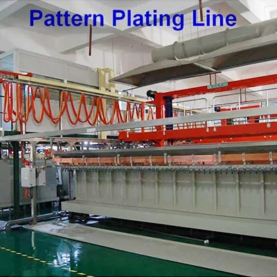
PCB pattern plating line
PCB solder mask expose machine
PCB pattern expose machine
Strip film etching line
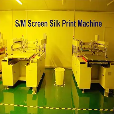
Solder mask screen silk print machine
Solder mask scrubbing line
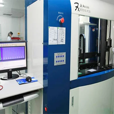
PCB Flying Probe Test (FPT)
Fully automatic exposure machine


