SMT330-X SMT Автоматический светодиодный светильник
Название: SMT330-X SMT Автоматическое светодиодное оборудование SMD
Происхождение: Китай
Сертифицировано: UL, CE, RoHS.
Поверхностная обработка: HASL/бессвинцовый HASL
Паяльная маска: зеленая, синяя, белая, красная и т. д.
Применение: PCB SMT LED SMD

SMT/DIP на 1~40 слоев обработки
Название: 1 ~ 40 слоев обработки чипов SMT/Dip
Происхождение: Китай
Сертифицировано: UL, CE, RoHS.
Материал:: ФР4/Подгонянный
Количество этажей:: 1–40 слоев по индивидуальному заказу.
Цвет паяльной маски:: Настроить. Черный. Зеленый. Красный. фиолетовый
Толщина меди: 1 унция/по индивидуальному заказу

Имя: SMT PCBA Прототип электроники
Происхождение: Китай
Сертифицировано: UL, CE, RoHS.
Толщина меди: 1-5 унций
Основной материал: FR4, высокий Tg FR4, общий Tg FR4, средний Tg FR4
Поверхностная обработка: HASL, OSP, иммерсионная лента
Толщина доски: по индивидуальному заказу

Сборка печатной платы SMT PCBA
Название: Сборка печатной платы SMT PCBA
Происхождение: Китай
Сертифицировано: UL, CE, RoHS.
Толщина меди: Индивидуальные
Цвет паяльной маски: зеленый, желтый, черный, синий, красный, белый, матовый зеленый.
Слой: 1-40
Базовый материал: FR-4/алюминий/керамика/cem-3/FR-1
Применение: Бытовая электроника
Толщина меди: 1/2 унции 1 унция 2 унции 3 унции

Печатная плата для обработки чипов SMT
Название: Печатная плата для обработки чипов SMT
Происхождение: Китай
Сертифицировано: UL, CE, RoHS.
Количество слоев: 1-40 слоев, 1-40 слоев.
Базовый материал: Fr4, алюминий
Толщина платы: по индивидуальному заказу
Поверхностная обработка: Иммерсионное золото/хасл/хасл без свинца
- PCB Assembly Capability
- PCB Assembly Equipment
- PCB Assembly Capability
Our SMT (Surface Mount Technology) Chip Processing service offers precise and efficient handling of surface mount chips for your electronic assembly needs. With our advanced equipment and skilled technicians, we provide professional chip processing solutions that meet the highest industry standards.
SMT chip involves the accurate placement, alignment, and soldering of surface mount chips onto printed circuit boards (PCBs). Whether you require small chip-scale packages or larger integrated circuits, our team has the expertise to handle a wide range of chip sizes and types.
Advantages of SMT chip processing:
- Precision placement: Our state-of-the-art pick-and-place machines ensure precise placement of surface mount chips onto PCBs. This results in accurate alignment of the chips, facilitating optimal electrical connections and reliable performance of your electronic devices.
- High-speed processing: SMT chip utilizes automated machinery to handle a large number of chips in a short period. This high-speed processing capability allows for efficient production cycles, reducing manufacturing time and costs.
- Miniaturization: Surface mount chips enable the miniaturization of electronic devices due to their smaller size compared to through-hole components. By utilizing SMT chip processing, you can design and produce compact and lightweight products without compromising functionality.
- Improved electrical performance: Surface mount chips offer improved electrical performance due to shorter trace lengths and reduced parasitic effects. This leads to enhanced signal integrity, lower electromagnetic interference, and improved overall functionality of your electronic products.
- Compatibility with advanced technologies: SMT chip supports the use of advanced chip technologies, such as microcontrollers, sensors, and integrated circuits. It enables the integration of complex functionalities and supports the latest advancements in the electronics industry.
| Item | Process Capability Parameter |
| Order Quantity | ≥1PC |
| Quality Grade | IPC-A-610 |
| Lead Time | 24 hours expedited service can be offered. 3- 4 days normally for PCBA prototype orders. We will give you an accurate lead time when we quote for you. |
| Size | 50*50mm~510*460mm |
| Board Type | Rigid PCB, Flexible PCB, metal core PCB |
| Min Package | 01005 (0.4mm*0.2mm) |
| Max Package | No limit |
| Mounting Accuracy | ±0.035mm(±0.025mm) Cpk≥1.0 (3σ) |
| Surface Finish | Lead/Lead-free HASL, Immersion gold, OPS, etc. |
| Assembly Types | Surface mount (SMT), Through-hole (DIP), Mixed Technology (SMT & Thru-hole) |
| Component Sourcing | Turnkey (All components sourced by PCBMay), Partial turnkey, Kitted/Consigned |
| BGA Package | BGA Dia. 0.14mm, BGA 0.2mm pitch |
| SMT Parts Presentation | Cut Tape, Partial reel, Reel,Tube, Tray, Laser-cut Stainless Steel |
| Cable Assembly | We supply custom cables, cable assemblies, wiring looms/harnesses and power leads for various industries including automotive, security, mining, medical and entertainment. |
| Stencil | Stencil with or without frame (offered free by PCBMay) |
| Quality Inspection | Visual inspection; AOI checking; BGA placement – X-RAY checking |
| SMT Capacity | 3 Million~4 Million Soldering Pad/day |
| DIP Capacity | 100 Thousand Pins/day |
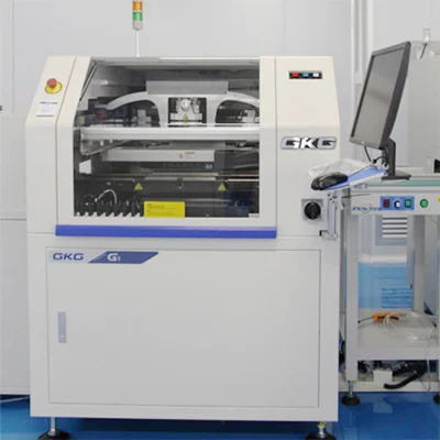
Automatic Solder Paste Printing Machine
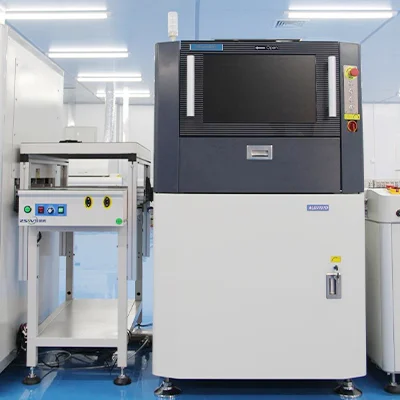
AOI Optical Inspection
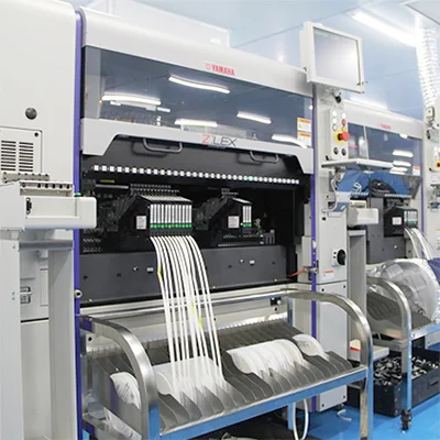
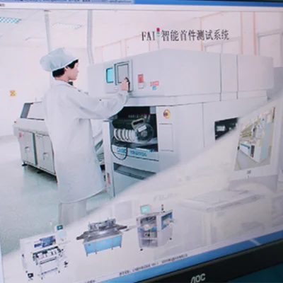
Smt High-Speed Placement Machine
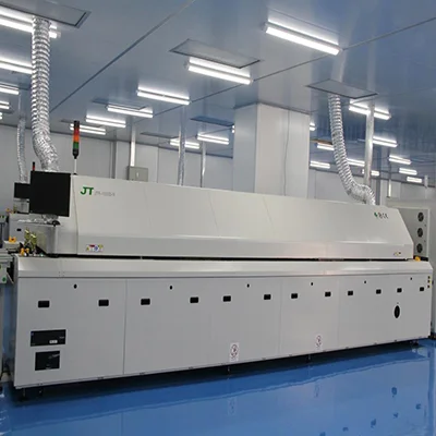
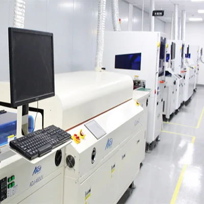
Nitrogen Reflow Soldering
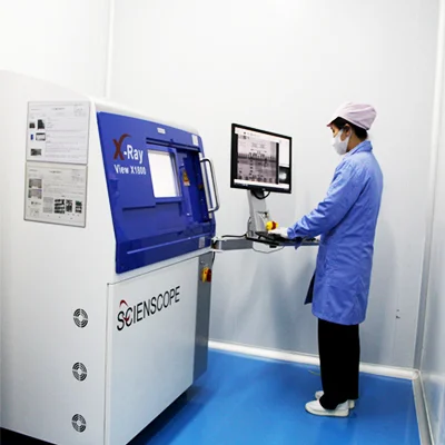
X-Ray
Three Anti-Paint Spraying Machine
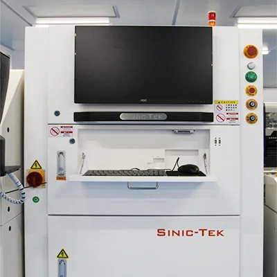
SPI Solder Paste Thickness Tester
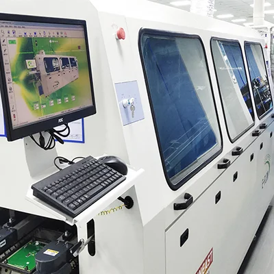
Automatic Wave Soldering Machine
First Article Inspection
| SMT capacity: 19 million points/day | ||
| Testing Equipment | X-RAY Nondestructive Tester, First Piece Tester, AOI Automatic Optical Tester, ICT Tester, BGA Rework Station | |
| Placement speed | Chip placement speed (at best conditions) 0.036 S/piece | |
| Mounted Component Specifications | Pasteable smallest package | |
| Minimum device accuracy | ||
| IC type chip accuracy | ||
| Mounted PCB Specifications | Substrate size | |
| Substrate thickness | ||
| throw rate | 1. Resistance-capacitance ratio 0.3% | |
| 2. IC type without throwing material | ||
| Board Type | POP/common board/FPC/rigid-flex board/metal substrate | |
| DIP daily production capacity | ||
| DIP plug-in production line | 50000 points/day | |
| DIP post welding production line | 20000 points/day | |
| DIP test production line | 50000pcs PCBA/day | |
| Assembly processing capability | ||
| The company has more than 10 advanced assembly production lines, dust-free and anti-static air-conditioning workshop, TP dust-free workshop, equipped with aging room, test room, functional test isolation room, advanced and perfect equipment, can carry out various product assembly, packaging, testing, Aging, etc. production. Monthly production capacity can reach 150,000 to 300,000 sets/month | ||
| PCBA processing capability | ||
| project | Mass processing capability | Small batch processing capability |
| Number of layers (max) | 2-18 | 20-30 |
| Plate type | FR-4, Ceramic Sheet, Aluminum Base Sheet PTFE, Halogen Free Sheet, High Tg Sheet | PTFE, PPO, PPE |
| Rogers,etc Teflon | E-65, ect | |
| Sheet mixing | 4 layers – 6 layers | 6th floor – 8th floor |
| biggest size | 610mm X 1100mm | / |
| Dimensional Accuracy | ±0.13mm | ±0.10mm |
| Plate thickness range | 0.2mm–6.00mm | 0.2mm–8.00mm |
| Thickness tolerance ( t≥0.8mm) | ±8% | ±5% |
| Thickness tolerance (t<0.8mm) | ±10% | ±8% |
| Media thickness | 0.076mm–6.00mm | 0.076mm–0.100mm |
| Minimum line width | 0.10mm | 0.075mm |
| Minimum spacing | 0.10mm | 0.075mm |
| Outer copper thickness | 8.75um–175um | 8.75um–280um |
| Inner layer copper thickness | 17.5um–175um | 0.15mm–0.25mm |
| Drilling hole diameter (mechanical drill) | 0.25mm–6.00mm | 0.15mm–0.25mm |
| Hole diameter (mechanical drill) | 0.20mm–6.00mm | 0.10mm–0.20mm |
| Hole Tolerance (Mechanical Drill) | 0.05mm | / |
| Hole tolerance (mechanical drill) | 0.075mm | 0.050mm |
| Laser Drilling Aperture | 0.10mm | 0.075mm |
| Plate thickness aperture ratio | 10:1 | 12:1 |
| Solder mask type | Photosensitive green, yellow, black, purple, blue, ink | / |
| Minimum Solder Mask Bridge Width | 0.10mm | 0.075mm |
| Minimum Solder Mask Isolation Ring | 0.05mm | 0.025mm |
| Plug hole diameter | 0.25mm–0.60mm | 0.60mm-0.80mm |
| Impedance tolerance | ±10% | ±5% |
| Surface treatment type | Hot air leveling, chemical nickel gold, immersion silver, electroplated nickel gold, chemical immersion tin, gold finger card board | Immersion Tin, OSP |


